Functional Material Measurement
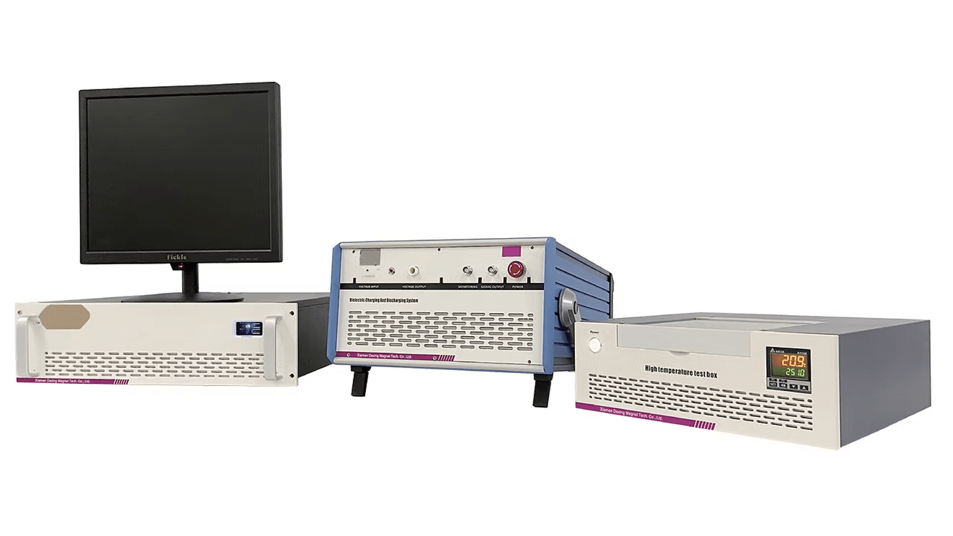
Dielectric Charging and Discharging System
Dexinmag dielectric charge and discharge test system is mainly used to study the high-voltage discharge performance of dielectric energy storage materials.
Product Overview
Dexinmag dielectric charge and discharge test system is mainly used to study the high-voltage discharge performance of dielectric energy storage materials. It enables researchers to characterise how quickly and efficiently dielectric films and ceramic capacitors release stored energy under different load and temperature conditions.
Features
- Strong scalability – can be connected to an external high-voltage amplifier or high-voltage DC power supply.
- High discharge current – discharge current can be detected by a current probe, up to 100A.
- Applicable to various sample tests – customized sample loading platform suitable for ceramic and thin-film sample testing.
- Data acquisition – collect data through an oscilloscope and directly calculate energy storage density.
- Signal source capability – can be used as a signal source to generate arbitrary waveforms.
- Variable temperature testing – supports temperature testing from RT to 250℃.
- Polarized material testing – suitable for polarized materials.
- Small parasitic capacitance and short switching time – uses a special high-voltage switch with single-pole double-throw structure, withstanding up to 10kV and providing very small parasitic capacitance.
- Two test modes – under-damping mode with discharge circuit short-circuited (no load resistance) and over-damping mode using precision non-inductive resistor as discharge load.
- Fatigue testing supported for repetitive charge/discharge cycling.
- Voltage and current capability – voltage up to 10kV and current up to 5mA (with optional high-voltage source modules).
Parameters
| Parameter | Specification |
|---|---|
| Equipment Model | DX-DSC-10KV |
| Current Probe Bandwidth | 120MHz |
| Peak Current | 0–100A, 150A |
| Current Acquisition Accuracy | 1mA |
| High Voltage Source Module | 3kV, 5kV, 10kV, 15kV optional (0–5mA) |
| Switch Application | 1 million cycles, withstand voltage 15kV |
| Temperature Control Range | 0–200℃ |
| Temperature Stability | 0.1℃ |
| Test Samples | Thin film, thick film, ceramic, glass |
| Note | Can be used with polarization equipment to test piezoelectric and dielectric materials. |
Test Circuit

In this circuit, the dielectric film is first charged to a specified voltage. The energy stored in the capacitor film is then discharged into a resistor load by closing the high-speed MOS high-voltage switch.
During discharge, the voltage change across the sample can be recorded by the detector. The discharge speed of dielectric materials depends on the resistance value of the load resistor.
To achieve different discharge conditions, resistors with different resistance values are installed in the test system. Users can select a single resistor or a combination of resistors to obtain the required resistance.
A high-voltage MOSFET switch is used to release the stored energy. The switch determines the maximum discharge speed and maximum charging voltage of the circuit.
System Structure
This test system consists of:
- Discharge acquisition circuit
- High-voltage amplifier or high-voltage DC power supply
- Control computer
During testing, the user selects a suitable resistor to determine the discharge speed, and the voltage on the test sample is automatically recorded by the computer.
Discharge Performance Example
As an example, the discharge behavior of a P(VDF-TrFE-CFE) terpolymer (63/37/7.5) film capacitor is analysed using the discharge circuit. Time-dependent voltage data is used to calculate the discharge energy density.
For a 1MΩ load resistor, the discharge energy density over time can be measured and compared with the energy density derived from the unipolar P–E loop. In this example, the film capacitance is approximately 1nF at 1kHz.
Because the polarization response of the terpolymer is nonlinear and frequency-dependent, the discharge behavior cannot be described by a simple RC constant. If RL > ESR, the discharge energy density can be expressed as:
Uc(t) = UD (1 − e^(−2t/τ)), where UD represents the discharge energy density.
Experimental Results
Using a 1nF capacitor and 1MΩ load resistor:
- 70% energy release time ≈ 0.6 ms (theoretical), measured ≈ 0.66 ms.
- 50% energy release time ≈ 0.35 ms (theoretical), measured ≈ 0.3 ms.
The differences arise due to the nonlinear dielectric constant at high electric fields (>100 MV/m), frequency-dependent dielectric response and lower ESR at high frequency or shorter discharge times.
Discharge Characteristics
For the same terpolymer film capacitor, discharge energy density can also be measured using different load resistances, such as RL = 100kΩ and RL = 1kΩ.
Reducing the load resistance shortens the discharge time, but the reduction is not linearly proportional due to nonlinear dielectric behavior and the complex frequency response of the material.